Technology
Photonic-Crystal Surface-Emitting Lasers Bring Innovation for Lasers
Currently, lasers utilized for smart mobility and smart manufacturing (LiDAR sensing and laser processing) are conventional broad-area semiconductor lasers, CO2 lasers and fiber lasers. However, these lasers have individual issues (click here for details). The key to fix the bottleneck is in Photonic-Crystal Surface-Emitting Lasers (PCSELs).
Operating Principle
Photonic-Crystal Surface-Emitting Lasers (PCSELs) operate at a singularity point (Γ-point, M-point, etc.) of two-dimensional (2D) photonic crystal, whose lattice (e.g., square, triangular) consists of two types of materials with a large refractive index contrast such as air/semiconductor. In this high-contrast lattice, not only fundamental Bloch waves, but also higher-order Bloch waves are coupled with each other to form a stable 2D standing wave (or resonant) mode. When the operation point is set at the singularity point of Γ-point, emission can be obtained from the surface of the photonic crystal; we named the laser a PCSEL to reflect this property.
Note that PCSELs are different from 2D distributed feedback (DFB) lasers, whose periodic structures have a smaller refractive index contrast such as semiconductor/semiconductor (namely, all semiconductor) and, thus, cannot facilitate coupling between all but the fundamental waves; this limitation of coupling prevents coherent 2D resonance of (most important) transverse-electric modes (TE) in square-lattice structures. This means PCSELs consisting of “all-semiconductors” does not work.
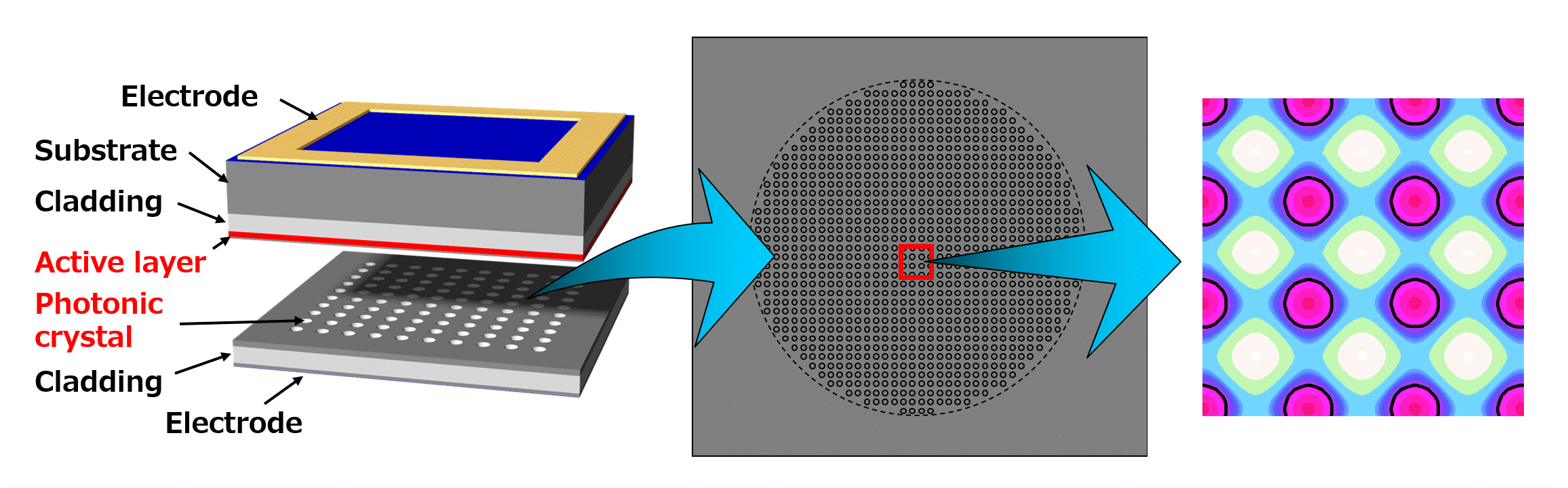
Feature of PCSELs
Owing to the 2D broad-area coherent oscillation, the brightness (or radiation brightness) B of PCSELs can be significantly increased. Here, the brightness B is defined as the optical power per unit area per unit solid angle, and is proportional to the device size S and is inversely proportional to the numbers of lateral modes m and n. In conventional broad-area Fabry-Perot semiconductor lasers, when S is increased to achieve high output power, multilateral-mode oscillation occurs and m and n are increased simultaneously. Thus, the brightness B cannot be increased. Similarly in vertical-cavity surface-emitting lasers, B cannot be increased due to the same reason. In PCSELs, however, since m and n can be kept very small (ideally zero) even though S increases, the brightness B can be significantly increased; 1-10 GW/cm2/sr, which are comparable to fiber lasers, are expected to be realized.
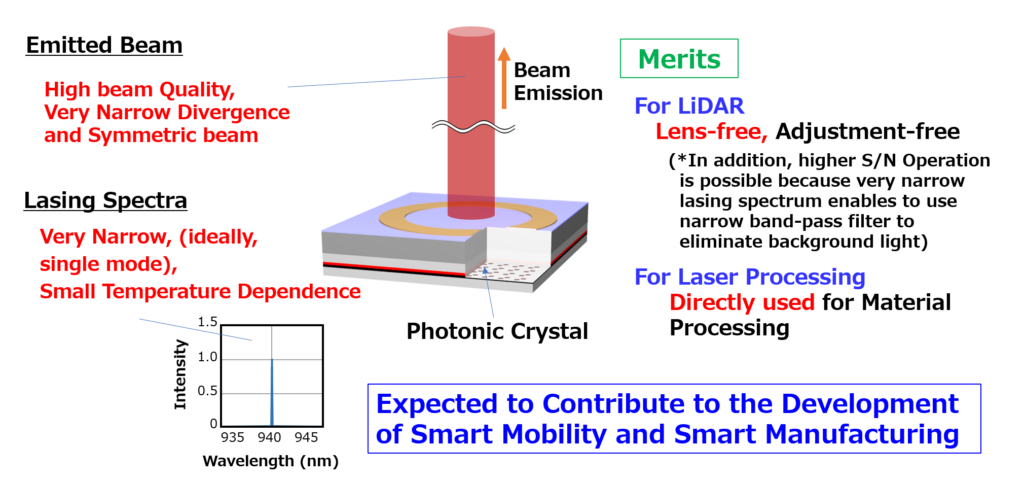
PCSELs have a very narrow divergence and symmetric beam. In addition, the lasing spectra is very narrow, ideally in a single mode, and their temperature dependence is much smaller than that of conventional broad area Fabry-Perot semiconductor lasers. Thus, the application merits of PCSELs are as follows: For LiDAR application, lens-free and adjustment free operation can be achieved. In addition, even higher S/N operation is possible. For laser processing, PCSEL can be directly used for laser processing. Thus, the PCSELs are expected to contribute to the development of smart mobility and smart manufacturing.
For Even Higher Brightness Operation
Impact of double lattice photonic crystal to realize high brightness operation
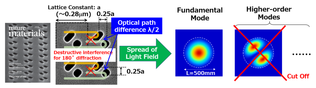
We recently introduced double-lattice structure, which we invented previously, where larger and smaller lattice points are combined with a shift of around 0.25a, where a is the lattice constant. In this photonic-crystal structure, the light waves diffracted by individual lattices have an optical-path difference of half wavelength. Thus, the destructive interference occurs for 180o degree diffraction. This destructive interference leads to the spreading of the light field. Because the antinode of the higher order mode becomes close to the edge of the device, the higher order mode becomes to be cut off. This leads to the high beam quality and high brightness operation.
Example of Device Performance
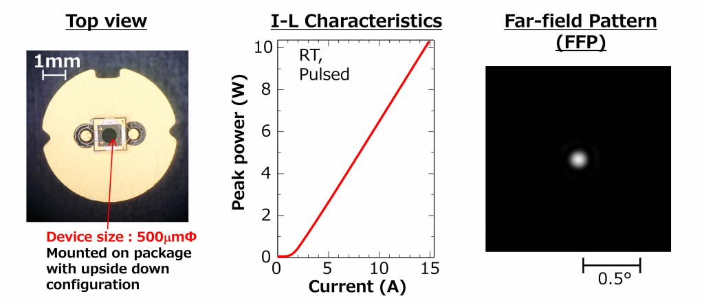
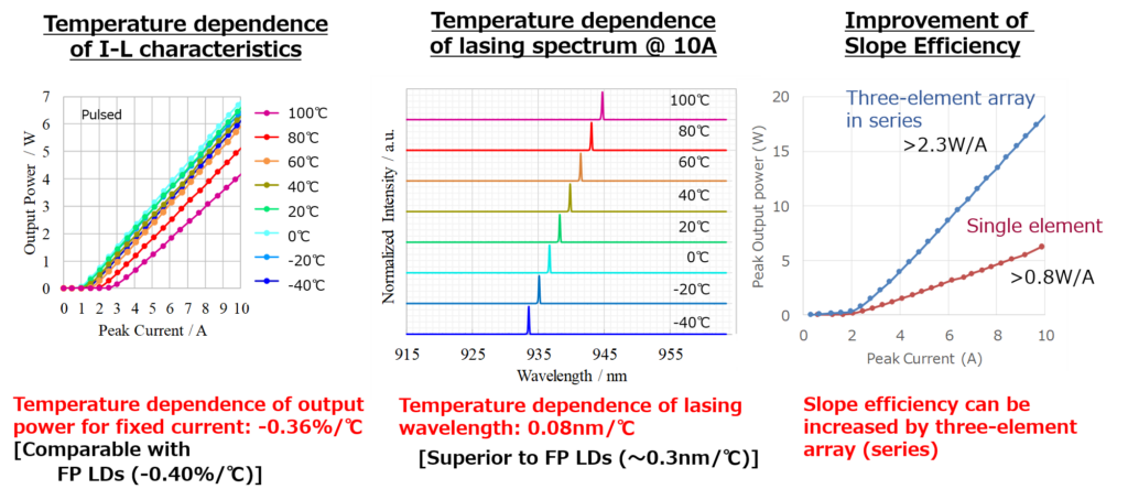
In the device mounted on a package in an upside down configuration, the output beam is emitted from the substrate side. From the I-L characteristic, 10W of output power is obtained with a high slope efficiency of 0.8W/A. A very narrow beam divergence of 0.1 degree has been achieved.
The detailed characteristics are shown below. The device operated successfully from -40 to 100oC (note that the measured temperature range is limited by measurement system), and the temperature dependence of output power at a fixed current injection is -0.36%/oC on average, which is comparable (or even superior) to that of Fabry-Perot semiconductor lasers. The temperature dependence of the lasing spectra shows that completely single mode oscillation is obtained from -40 to 100oC. The temperature dependency of lasing wavelength is as small as 0.08nm/oC, which is superior to FP LDs. Improvement of the slope efficiency can be achieved by introducing a three-element array in series.
_
_
General Recipe to Realize PCSELs with
100-W-to-1-kW Single-Mode Operation
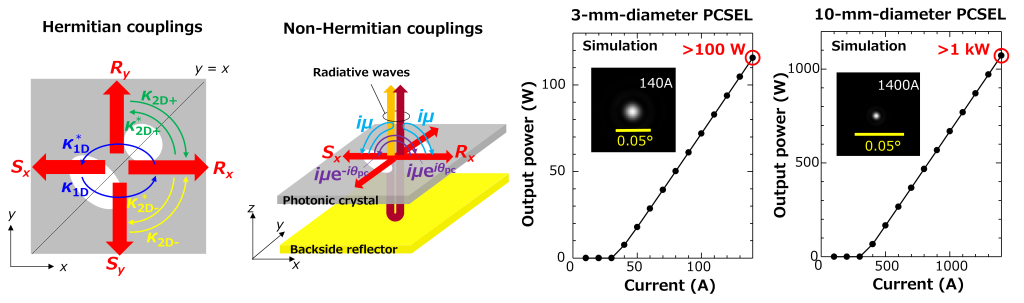
By further expanding the concept of the double-lattice photonic crystal mentioned above, we have recently derived a general recipe for ultra-large-area single-mode operation of PCSELs. Here, we have considered not only the optical couplings without energy loss (=Hermitian couplings) but also the couplings with energy loss via vertical radiation (=non-Hermitian couplings) as shown in the figure below. We have proven that the radiation loss of the higher-order modes can be increased more than those of the fundamental mode through a reasonable reduction of both coupling coefficients, while the balance between the two coefficients should be maintained to ensure stable single-mode lasing. Furthermore, we have successfully revealed that PCSELs with double-lattice photonic crystals and backside reflectors allow the arbitrary control of both Hermitian and non-Hermitian optical coupling coefficients, enabling 100-W-to-1-kW-class single-mode lasing with an ultra-large lasing diameter (≥3~10 mm).
Highly functional PCSELs (Beam Scanning)
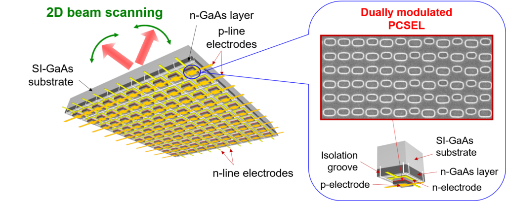
As an example of high functionality, non-mechanical beam scanning has been realized based on PCSEL technology.
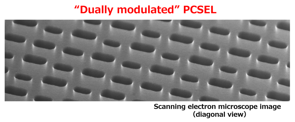
This function is important for an ultra-compact, reliable, stable LiDAR system. We recently invented, so called, ‘dually modulated’ PCSEL, where the lattice-point sizes and positions are simultaneously modulated. This enable to include the information of the emission direction. A chip for electrical 2D beam scanning based on dually modulated photonic crystals has been realized by integrating 10×10 different dually modulated PCSELs in a 2D matrix, where individual PCSELs can be driven independently.
Publications
[1] Imada, M.; Noda, S.; Chutinan, A.; Tokuda, T.; Murata, M.; Sasaki, G. Coherent two-dimensional lasing action in surface-emitting laser with triangular-lattice photonic crystal structure. Applied Physics Letters 1999, 75, 316–318.
[2] Noda, S.; Yokoyama, M.; Imada, M.; Chutinan, A.; Mochizuki, M. Polarization mode control of two-dimensional photonic crystal laser by unit cell structure design. Science 2001, 293, 1123–1125.
[3] Miyai, E.; Sakai, K.; Okano, T.; Kunishi,W.; Ohnishi, D.; Noda, S. Lasers producing tailored beams. Nature 2006, 441, 946.
[4] Sakai, K.; Miyai, E.; Noda, S. Coupled-wave model for square-lattice two-dimensional photonic crystal with transverse-electric-like mode. Applied Physics Letters 2006, 89, 021101.
[5] Sakai, K.; Miyai, E.; Noda, S. Two-dimensional coupled wave theory for square-lattice photonic-crystal lasers with TM-polarization. Optics Express 2007, 15, 3981.
[6] Matsubara, H.; Yoshimoto, S.; Saito, H.; Yue, J.; Tanaka, Y.; Noda, S. GaN photonic-crystal surface-emitting laser at blue-violet wavelengths. Science 2008, 319, 445–447.
[7] Sakai, K.; Yue, J.; Noda, S. Coupled-wave model for triangular-lattice photonic crystal with transverse electric polarization. Optics Express 2008, 16, 6033.
[8] Kurosaka, Y.; Iwahashi, S.; Liang, Y.; Sakai, K.; Miyai, E.; Kunishi, W.; Ohnishi, D.; Noda, S. On-chip beam-steering photonic-crystal lasers. Nature Photonics 2010, 4, 447–450.
[9] Sakai, K.; Miyai, E.; Noda, S. Coupled-wave theory for square-lattice photonic crystal lasers with TE polarization. IEEE Journal of Quantum Electronics 2010, 46, 788.
[10] Liang, Y.; Peng, C.; Sakai, K.; Iwahashi, S.; Noda, S. Three-dimensional coupled-wave model for square-lattice photonic crystal lasers with transverse electric polarization: A general approach. Physical Review B 2011, 84, 195119.
[11] Liang, Y.; Peng, C.; Sakai, K.; Iwahashi, S.; Noda, S. Three-dimensional coupled-wave analysis for square-lattice photonic crystal surface emitting lasers with transverse-electric polarization: finite-size effects. Optics Express 2012, 20, 15945.
[12] Peng, C.; Liang, Y.; Sakai, K.; Iwahashi, S.; Noda, S. Three-dimensional coupled-wave theory analysis of a centered-rectangular lattice photonic crystal laser with a transverse-electric-like mode. Physical Review B 2012, 86, 035108.
[13] Commercially available from Hamamatsu Photonics https://www.hamamatsu.com/jp/en/product/lasers/semiconductor-lasers/pcsels/index.html
[14] Liang, Y.; Peng, C.; Ishizaki, K.; Iwahashi, S.; Sakai, K.; Tanaka, Y.; Kitamura, K.; Noda, S. Three-dimensional coupled-wave analysis for triangular-lattice photonic-crystal surface-emitting lasers with transverse-electric polarization. Optics Express 2013, 21, 565.
[15] Hirose, K.; Liang, Y.; Kurosaka, Y.; Watanabe, A.; Sugiyama, T.; Noda, S. Watt-class high-power, high-beam-quality photonic-crystal lasers. Nature Photonics 2014, 8, 406–411.
[16] Liang, Y.; Okino T.; Kitamura, K.; Peng, C.; Ishizaki, K.; Noda, S. Mode stability in photonic-crystal surface-emitting lasers with large κ1DL. Applied Physics Letters 2014, 104, 021102.
[17] Noda, S.; Kitamura, K.; Okino, T.; Yasuda, D; Tanaka Y. Photonic-crystal surface-emitting lasers: Review and introduction of modulated-photonic crystals. IEEE Jounral of Selected Topics on Quantum Electronnics 2017, 23, 4900107 (Invited Paper).
[18] Yoshida, M.; De Zoysa, M.; Ishizaki, K.; Tanaka, Y.; Kawasaki, M.; Hatsuda, R.; Song, B.-S.; Gelleta, J.; Noda, S. Double-lattice photonic-crystal resonators enabling high-brightness semiconductor lasers with symmetric narrow-divergence beams. Nature Materials 2019, 18, 121–128.
[19] Inoue, T.; Morita, R.; Yoshida, M.; De Zoysa, M,; Tanaka, Y.; Noda, S. Comprehensive analysis of photonic-crystal surface-emitting lasers via time-dependent three-dimensional coupled-wave theory. Physical Review B 2019, 2019, 99, 035308.
[20] Sakata, R.; Ishizaki, K.; De Zoysa, M.; Fukuhara, S.; Inoue, T.; Tanaka, Y.; Iwata, K.; Hatsuda, R.; Yoshida, M.; Gelleta, J.; Noda, S. Dually modulated photonic crystals enabling high-power high-beam-quality two-dimensional beam scanning lasers. Nature Communications 2020, 11, 3487.
[21] Morita, R.; Inoue, T.; De Zoysa, M.; Ishizaki, K.; Noda, S. Photonic-crystal lasers with two-dimensionally arranged gain and loss sections for high-peak-power short-pulse operation. Nature Photonics 2021, 15, 311.
[22] Yoshida, M.; De Zoysa, M.; Ishizaki, K.; Kunishi, W.; Inoue, T.; Izumi, K.; Hatsuda, R.; Noda, S. Photonic-crystal lasers with high-quality narrow-divergence symmetric beams and their application to LiDAR. Journal of Physics: Photonics 2021, 3, 022006.
[23] Inoue, T.; Yoshida, M.; Gelleta, J.; Izumi, K.; Yoshida, K.; Ishizaki, K.; De Zoysa, M.; Noda, S. General recipe to realize photonic-crystal surface emitting lasers with 100-W-to-1-kW single-mode operation. Nature Communications 2022, 13, 3262.
[24] Inoue, T.; Morita, R.; Nigo, K.; Yoshida, M.; De Zoysa, M,; Ishizaki, K.; Noda, S. Self-evolving photonic crystals for ultrafast photonics. Nature Communications 2023, 14, 50.
[25] Inoue, T.; Kim, T.; Katsuno, S.; Moritam R.; Yoshida, M.; De Zoysa, M,; Ishizaki, K.; Noda, S. Measurement and numerical analysis of intrinsic spectral linewidths of photonic-crystal surface-emitting lasers. Applied Physics Letters 2023, 122, 051101.
[26] Sakata, R.; Ishizaki, K.; De Zoysa, M.; Kitamura, K.; Inoue, T.; Gelleta, J.; Noda, S. Photonic-crystal surface-emitting lasers with modulated photonic crystals enabling 2D beam scanning and various beam pattern emission, Applied Physics Letteers -Perspective- 2023, 122, 130503.
[27] Yoshida, M.; Katsuno, S.; Inoue, T.; Gelleta, J.; Izumi, K.; De Zoysa, M.; Ishizaki, K.; Noda, S. High-brightness scalable continuous-wave single-mode photonic-crystal laser. Nature 2023 (DOI: 10.1038/s41586-023-06059-8).
In addition, there are more than 570 related publications in international journals and international conferences. Total citations exceed 32,000.
Patents
[1] S. Noda, G. Sasaki, et al., patent No. JP3983933
[2] S. Noda, M. Yokoyama, et al., patent No. JP4484134, CN100433473C, KR100792078B1, DE602004015090D1, EP1610427B1, CA2521005C
[3] K. Sakai, S. Noda, et al., patent No. JP4793820, TWI426673B, US7936801B2
[4] K. Otsuka, S. Noda, et al., patent No. JP5072402, US7656925B2
[5] S. Noda, S. Iwahashi, et al., patent No. JP5794687, US8619830B2
[6] S. Noda, T. Sakaguchi, et al., patent No. JP5874947
[7] S. Noda, T. Okino, et al., patent No. JP6080941, US9531160B2, CN105191029B, EP2966737B1
[8] K. Hirose, S. Noda, et al., patent No. JP6213915, US9583914B2
[9] S. Noda, Y. Tanaka, et al., patent No. JP6860175, DE112017001040T8, CN108701965B, US10461502B2
[10] S. Noda, H. Kitagawa, et al., patent No. JP6865439, CN108028511B, US10389086B2
In addition, there are more than 122 related patents.